[Read Paper] The N3XT Approach to Energy-Efficient Abundant-Data Computing
- The N3XT Approach to Energy-Efficient Abundant-Data Computing
The N3XT Approach to Energy-Efficient Abundant-Data Computing
This paper introduces Nano-Engineered Computing Systems Technology (N3XT) approach which emerges device (logic and memory) nanotechnologies and their dense 3-D integration with fine-grained connectivity to immerse computing in memory and new logic devices (such as carbon nanotube field-effect transistors for implementing high-speed and low-energy logic circuits) as well as high-density nonvolatile memory (such as resistive memory), and amenable to ultra-dense (monolithic) 3-D integration of thin layers of logic and memory devices that are fabricated at low temperature.
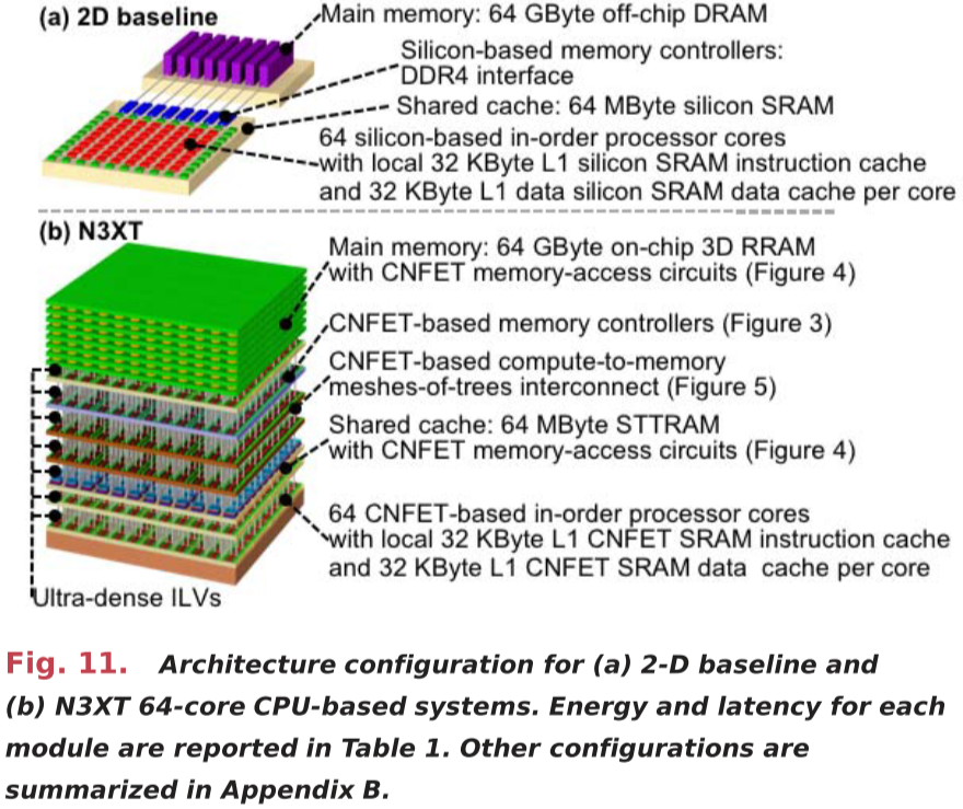
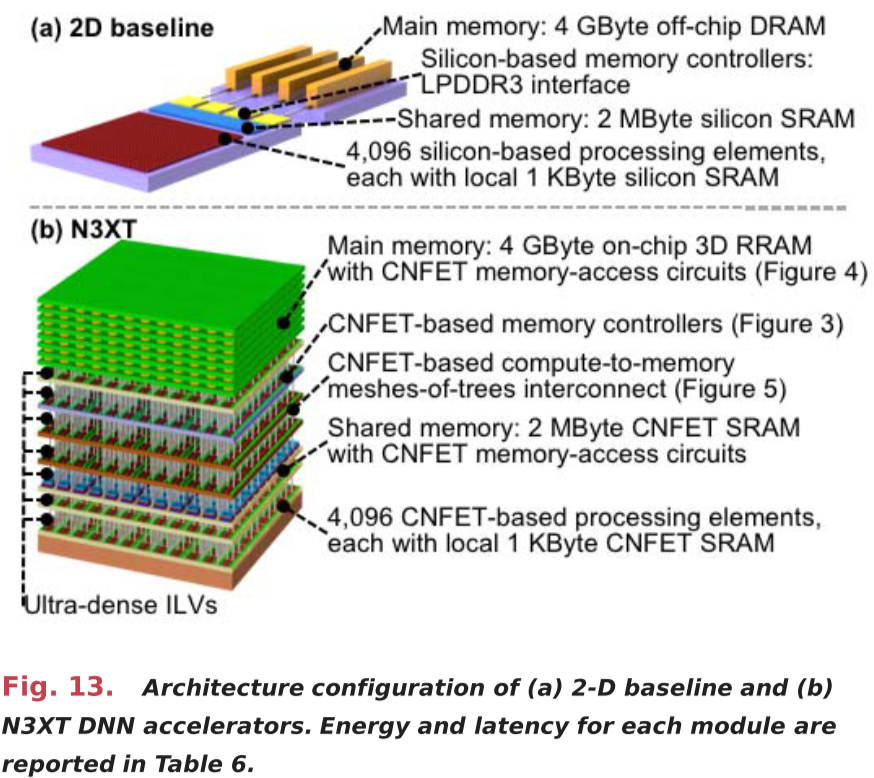
N3XT Architecture
Tiers are linked using nanoscale ILVs. The high density of ILVs is essential to achieving the massive benefits in application energy and execution time.
Via
Tiers are linked using nanoscale ILVs. ILVs provide a substantially higher number of connections per unit area (versus TSVs), supporting wider and many more concurrent accesses to memory.
Compute tiers
A compute tier supports CPU cores, GPUs, domain-specific accelerators, and combinations thereof.
Memory tiers
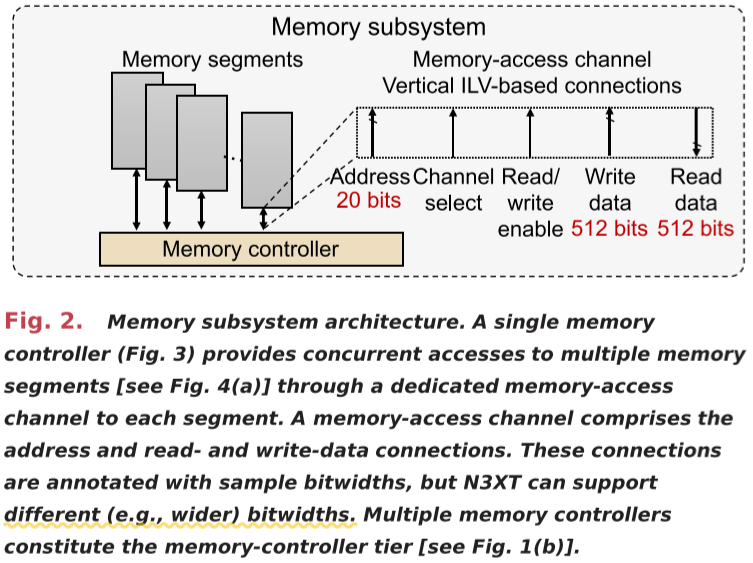
Each memory tier in the memory subsystem can be one of the following:
- a memory-controller tier;
- a memory-access-circuits (sense amplifiers, selector, address decoders, and so on) tier;
- a memory-cells tier.
Memory-controller tier
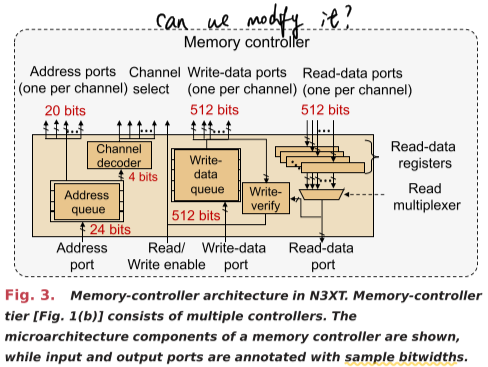
A memory controller consists the following:
- An address queue to buffer incoming memory-access requests.
- A write-data queue to temporarily store incoming data.
- A set of read-data registers, one per memory-access channel.
- Logic blocks—channel decoder and read multiplexer—for data or address routing.
- A write-verify module, where the written data are immediately read and compared with data stored in the write-data queue to ensure successful operation.
Memory-access-circuits tier (sense amplifiers, selector, address decoders, and so on)
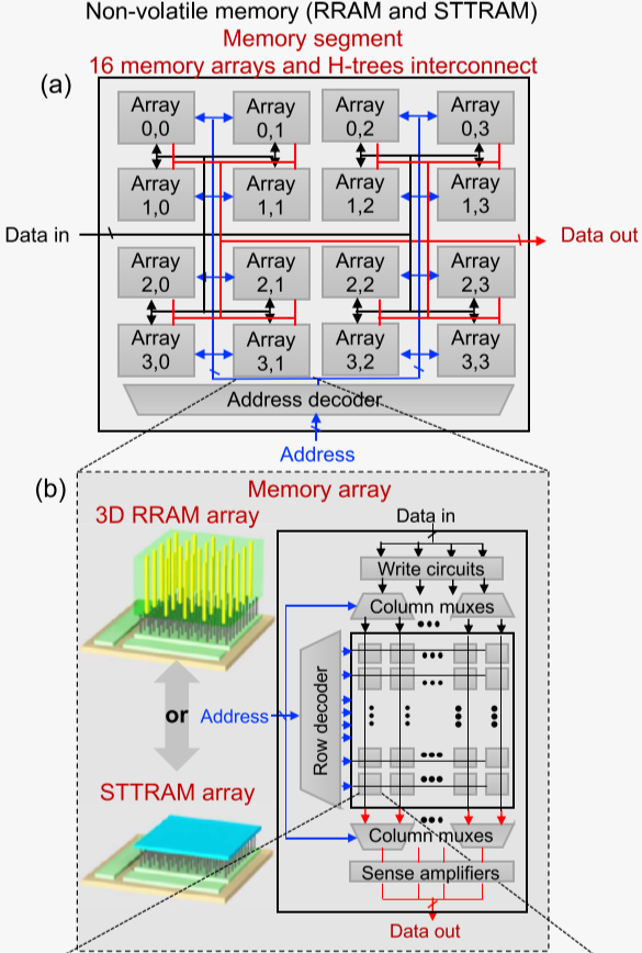
Memory-cells tier
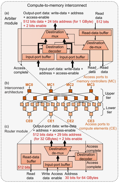
Compute-to-memory interconnect
Compute-to-memory interconnect tiers support for uniform memory access (UMA) so that each compute unit has the same access latency to each memory location.
Using the meshes of trees (MoTs) interconnect scheme as it provides lower access latency and energy, as well as higher bandwidth to memory compared with other schemes. The MoT interconnect scheme is defined by a set of router and arbiter modules. Each compute element is linked to a separate binary tree of router modules, with one leaf per memory controller.
Cooling tiers
Cooling tiers may include advanced cooling solutions, such as phase-change materials and 2-D materials that laterally spread the heat to the edge of the chip, alleviate thermal hot spots, and decrease the overall operating temperature.
N3XT Technology Foundations
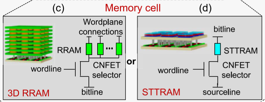
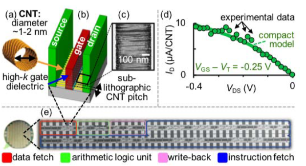
Energy-efficient carbon nanotube FETS (CNFETs)
CNFETs use multiple (parallel) carbon nanotubes (CNTs) for transistor channel.
On-chip nonvolatile memories
On-chip nonvolatile memories include spin-transfer torque magnetic RAM (STTRAM or STT-MRAM) and metal–oxide RRAM—they offer tradeoffs in terms of latency, energy, density, retention, and endurance when designing the memory hierarchy.
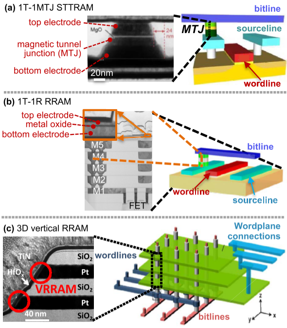
STTRAM:
- slower write latency and higher energy
- read latency and energy comparable
- denser
RRAM:
- naturally enables bit-cost-scalable vertical 3D RRAM, bringing greater storage density
- an RRAM cell can store a single bit or multiple bits
Architecture Evaluation Methodology
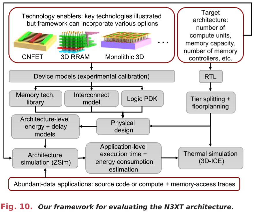
We have customized design and simulation tools from device to architecture levels and assembled them into an exploration framework.
Circuit modeling using CNFETs
CNFET PDK with standard synthesis and place-and-route tools.
The variation-aware nano-system design kit generates CNFET PDKs by extracting the standard-cell layouts from a SiFET PDK and using the CNFET model to replace each SiFET in the layouts with a CNFET of the same gate pitch and width to maintain the same footprint.
- Parasitic resistances and capacitances for logic gates and interconnects: Mentor Graphics Calibre xACT 3-D
- power: Cadence Spectre
- timing: Cadence Liberate
Modeling the STTRAM and RRAM
- Cell level parameters from experimental data:
- ON-and OFF-resistances
- read/write currents and voltages
- cell area
- write latency
- Digital blocks for memory-access circuits (including address, row, and column decoders): CNFET PDK
- The analog components (including column multiplexers, sense amplifiers, pulse generators, write drivers, and word-line drivers): SPICE
- access latency and energy for a given memory segment: NVSim
Interconnect modeling with monolithic 3D integration
- synthesize a gate-level netlist: CNFET PDK
- place-and-route: Synopsys IC Compiler
Architectural simulation
- The application-level execution time and energy consumption: Combined ZSim with TETRIS
- Parameters:
- a number of compute units as well as their type, operating frequency, active, and idle energy;
- capacity, access latency, and energy of local (one per compute unit) and shared (among all compute units) memories
- compute-to-memory interconnect latency and energy per access (to account for UMA);
- capacity, access latency, and energy of main memory, number of access channels to memory, and bandwidth per channel.
For a given application, simulation produces the following outputs:
- a number of operations executed per compute unit;
- a number of cycles consumed in memory accesses;
- a number of memory accesses (read and write) to local, global, and main memory;
- energy consumed in each compute unit when executing instructions and also when idle (due to memory access);
- energy consumed in local, global, and main memories;
- execution time and the corresponding breakdown into compute and memory-access times;
- a number of reads and writes to each memory word in main memory.
Thermal simulation
- operating temperatures for N3XT and other architecture configurations: 3D-ICE
Technology Alternatives for Implementing N3XT
Impact of Compute-to-Memory Connectivity
- vary the number of compute-to-memory connections, i.e., vertical connections between:
- the compute tier and the compute-to-memory-interconnect tiers;
- the compute-to-memory-interconnect tiers and the memory-controller tier;
- the memory-controller tier and the memory-access-circuits tier of the nonvolatile 3-D RRAM
- vary
- the number of channels in each memory controller (1– 16 channels per controller),
- the bitwidth in each channel within the memory controller (64–512 bits per channel),
- the bitwidth in compute-to-memory interconnect (64–512 bits per channel).
- assume that:
- memory-access circuits are connected to the nonvolatile memory cells with ILVs
- compute units, compute-to-memory interconnect, memory controllers, and memory-access circuits are designed using CNFETs for all analyzed configurations.
Impact of Alternative Logic Devices in the Compute Tier
improved logic devices in the compute tier have a notable impact for more compute-bound work-loads.
Impact of Alternative Logic Devices in the Upper Tiers
Memory-bound workloads are more sensitive to such changes.
RRAM Endurance Resiliency
Optimizations on different levels
Device-level optimizations
Such as tuning cell geometries, changing RRAM materials, and tuning the write latency and current, can increase RRAM endurance
Architectural optimizations
Such as reducing operating frequency, the number compute units, and RRAM connectivity, can improve system lifetime.
However, such changes may reduce the resulting EDP benefits of N3XT.
Avoiding unnecessary writes to RRAM
It is an effective approach to increase lifetime considerably.
an architecture that maps the smaller data structures to SRAM and the larger data structures to RRAM.
The ENDURER technique
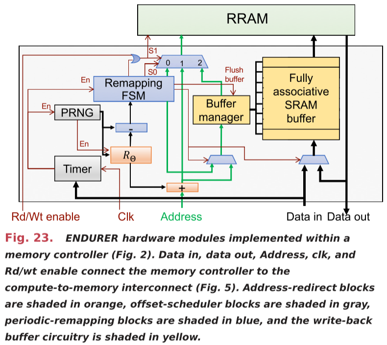
Address redirect
Address redirect maps each incoming memory address (A) into a different address ( ¯A) by adding offset Θ
Offset scheduler
Offset scheduler selects Θ as a random value uniformly distributed in {0, 1,…,M−1} every T seconds.
Periodic remapping
Periodic remapping cyclically shifts the contents of the entire memory.
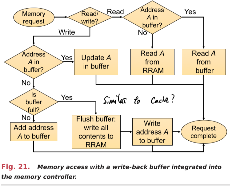
The write-back buffer
The write-back buffer is a fully associative SRAM of size S words that places an upper bound on the number of writes to each RRAM word.
This can reduce peak writes per word.
Terms
Via Types: ILVs & TSVs
- TSVs: through-silicon vias. TSV pitch is on the order of 3-5 μm at the 14- and 7-nm technology nodes.
- ILVs: interlayer vias. ILV pitches are 80 and 40nm respectively at the 14- and 7-nm technology nodes.
Others
- EDP: energy-delay product. Defined as the product of application energy consumption and execution time.
- MoTs: meshes of trees
Logic Layer Types: SiFET & CNFETs
- SiFET & CNFETs: silicon FET, energy-efficient carbon nanotube FETs
Memory Types: RRAM & STTRAM
- RRAM & STTRAM: metal-oxide resistive RAM, spin-torque transfer RAM